


Texas Instruments TPS65917/TPS65917-Q1 Power Management IC (PMIC)
Texas Instruments TPS65917/TPS65917-Q1 Power Management IC (PMIC) integrates five configurable step-down converters with up to 3.5A of output current to power the processor core, memory, I/O, and preregulation of LDOs. The step-down converters are synchronized to an internal 2.2MHz clock to improve the EMC performance of the device. The GPIO_3 pin allows the step-down converters to synchronize to an external clock, allowing multiple devices to synchronize to the same clock. This feature improves system-level EMC performance. The device also contains five LDOs to power low-current or low-noise domains. The power-sequence controller uses one-time programmable (OTP) memory to control the power sequences. This memory also holds default configurations such as output voltage and GPIO configurations. The OTP is factory-programmed to allow start-up without any software required. Most static settings can be changed from the default through SPI or I2C to configure the device to meet many different system needs. The TPS65917-Q1 devices are AEC-Q100 qualified for automotive applications.
Features
- Qualified for automotive applications
- AEC-Q100 qualified with the following results:
- Device temperature grade 2: –40°C to 105°C ambient operating temperature range
- Device HBM classification level 2
- Device CDM classification level C4B
- System voltage range from 3.135V to 5.25V
- Low-power consumption:
- 20µA in OFF mode
- 90µA in sleep mode with two SMPSs active
- Five step-down Switched-Mode Power Supply (SMPS) regulators:
- 0.7 to 3.3V output voltage range in 10 or 20mV steps
- Two SMPS regulators with 3.5A capability, with the ability to combine into 7A output in dual-phase configuration, with differential remote sensing (Output and Ground)
- Three other SMPS regulators with 3A, 2A, and 1.5A capabilities
- Dynamic Voltage Scaling (DVS) control and output current measurement in 3.5A and 3A SMPS regulators
- Hardware and software controlled Eco-mode™ supplying up to 5mA
- Short-circuit protection
- Power-Good indication (voltage and overcurrent indication)
- Internal Soft-Start for In-rush current limitation
- Ability to synchronize to an external clock between 1.7MHz and 2.7MHz
- Five Low-Dropout (LDO) linear regulators
- 0.9 to 3.3V output range in 50mV steps
- Two with 300mA capability and bypass mode
- One with 100mA capability and capable of low-noise performance up to 50mA
- Two other LDOs with 200mA current capability
- Short-circuit protection
- 12-Bit Sigma-Delta General-Purpose ADC (GPADC) with 8 input channels (2 external)
- Thermal monitoring with a high-temperature warning and thermal shutdown
- Power sequence control:
- Configurable power-up and power-down sequences (OTP)
- Configurable sequences between the SLEEP and ACTIVE state transition (OTP)
- Three digital output signals that can be included in the startup sequence
- Selectable control interface:
- One SPI for resource configurations and DVS control
- Two I2C interfaces:
- One dedicated for DVS control
- One general purpose I2C interface for resource configuration and DVS control
- OTP Bit-Integrity error detection with options to proceed or hold power-up sequence and RESET_OUT release
- Package option:
- 7mm × 7mm 48-pin VQFN with 0.5mm pitch
Applications
- Automotive digital cluster
- Automotive Advanced Driver Assistance System (ADAS)
- Automotive navigation systems
Associated Product
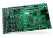
Texas Instruments TPS65917EVM PMIC Evaluation Module (EVM)
Evaluates the features and capabilities of the TPS65917-Q1, a power management IC (PMIC).
Videos
Functional Block Diagram
")
Đã phát hành: 2017-09-28
| Đã cập nhật: 2022-06-21