


Renesas Electronics RC22504A & RC32504A FemtoClock® 2 Synthesizers
Renesas Electronics RC22504A and RC32504A FemtoClock® 2 Synthesizers are designed to be placed adjacent to a PHY, switch, ASIC, or FPGA that requires several reference clocks with less than 100fs (max) jitter performance. The RC22504A acts as a frequency synthesizer to locally generate the reference clock or as a DCO for frequency margining or OTN clock applications. The RC32504A can act as a frequency synthesizer to locally generate the reference clock, a jitter attenuator to perform local clean-up and/or frequency translation of a centrally-supplied reference, a Synchronous Ethernet equipment clock to perform passband filtering and clean-up of network-supplied references, or as a DCO for frequency margining or OTN clock applications. These devices are members of Renesas' high-performance FemtoClock2 family.
The Renesas Electronics RC22504A and RC32504A FemtoClock 2 Synthesizers are offered in a Quad Flat No-Lead (QFN) package with an exposed pad for improved thermal performance.
Features
- RC32504A
- Jitter below 100fs RMS (10kHz to 20MHz)
- Compliant with ITU-T G.8262 for synchronous Ethernet/OTN (EEC/OEC) and ITU-T G.8262.1 for enhanced synchronous Ethernet/OTN
(eEEC/eOEC) - PLL core consists of fractional-feedback Analog PLL (APLL) which can optionally be steered by a Digital PLL (DPLL)
- Operates from a 25MHz to 80MHz crystal or XO
- APLL frequency independent of input/crystal frequency
- Operates as a frequency synthesizer, jitter attenuator, synchronous equipment slave clock or Digitally Controlled Oscillator (DCO)
- DPLL loop filter programmable from 0.1Hz to 12kHz
- DCO has tuning granularity of < 1ppt
- Programmable input buffer supports HCSL, LVDS, or two LVCMOS with no external terminations needed
- Input frequencies: 1MHz to 800MHz (250MHz for LVCMOS)
- Reference monitor qualifies/disqualifies input clock
- Programmable status output
- 4 differential/8 LVCMOS outputs
- Any frequency from 10MHz to 1GHz (180MHz for LVCMOS)
- Programmable output buffer supports HCSL (DC-coupled), LVDS/LVPECL/CML (AC-coupled) or two LVCMOS
- Differential output swing is selectable: 400mV to 800mV
- Output Enable input with programmable effect
- Supports up to 1MHz I2C or up to 20MHz SPI serial processor port
- Can configure itself automatically after reset through internal customer-definable One-Time Programmable (OTP) memory with up to four different configurations
- 4mm x 4mm QFN-24 package
- RC22504A
- Jitter as low as 64fs RMS maximum (10Hz to 20MHz)
- PLL core consists of fractional-feedback Analog PLL (APLL)
- Operates from a 25MHz to 80MHz crystal or XO
- APLL frequency independent of input/crystal frequency
- Operates as a frequency synthesizer or Digitally Controlled Oscillator (DCO)
- DCO has tuning granularity of < 1ppb
- Programmable status output
- 4 differential / 8 LVCMOS outputs
- Any frequency from 10MHz to 1GHz (180MHz for LVCMOS)
- Programmable output buffer supports HCSL (DC-coupled), LVDS/LVPECL/CML (AC-coupled), or two LVCMOS
- The differential output swing is selectable from 400mV to 800mV
- Output Enable input with programmable effect
- Supports up to 1MHz I2C or up to 20MHz SPI serial processor port
- Can configure itself automatically after reset via internal customer-definable One-Time Programmable (OTP) memory with up to four
different configurations - 4mm x 4mm QFN-24 package
Applications
- RC32504A
- Synchronous Ethernet/OTN equipment
- Reference clock generator for 100Gbps/400Gbps PHYs or switches
- Adjustable OTN clock reference for OTU3/OTU4 mappers
- Reference clock for programmable FiberOptic Modules
- RC22504A
- Reference clock generator for 100Gbps / 400Gbps PHYs or switches
- Adjustable OTN clock reference for OTU3 / OTU4 mappers
- Reference clock for programmable FiberOptic Modules
Development Tools
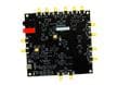
Renesas Electronics RC22504A Evaluation Kit
Used for the RC32504A and RC22504A point-of-use jitter attenuator and clock generators.
Block Diagrams

Package Outline

Đã phát hành: 2021-04-26
| Đã cập nhật: 2022-03-11