


Texas Instruments SN74AVC1T45/SN74AVC1T45-Q1 Bus Transceiver
Texas Instruments SN74AVC1T45/SN74AVC1T45-Q1 Bus Transceiver is a single-bit, non-inverting bus transceiver using two configurable power-supply rails. The SN74AVC1T45/SN74AVC1T45-Q1 is operational with VCCA/VCCB as low as 1.08V. The A port is designed to track VCCA. VCCA accepts any supply voltage from 1.08V to 3.6V. The B port is designed to track VCCB. VCCB accepts any supply voltage from 1.08V to 3.6V. This feature allows universal low-voltage, bidirectional translation between either 1.2V, 1.5V, 1.8V, 2.5V, and 3.3V voltage nodes.
The SN74AVC1T45/SN74AVC1T45-Q1 is designed for asynchronous communication between two data buses. The logic levels of the direction-control (DIR) input activate either the A-port outputs or the B-port outputs. When the B-port outputs are activated, the device transmits data from the A bus to the B bus. If the A-port outputs are activated, the device transmits from the B bus to the A bus. The input circuitry on both A and B ports is always active. It must apply a logic HIGH or LOW level to prevent excess ICC and ICCZ.
The Texas Instruments SN74AVC1T45/SN74AVC1T45-Q1 is designed so that the DIR input is powered by VCCA. This device is fully specified for partial-power-down applications using Ioff. When powered down, the Ioff circuitry disables the outputs, preventing damage to the current backflow. The VCC isolation feature is designed so that if either VCC input is at GND, both ports are in the high-impedance state. NanoFree package technology uses the die as the package and is a breakthrough in IC packaging concepts.
Features
- Available in the Texas Instruments NanoFree™ package
- A fully configurable dual-rail design allows each port to operate over the full 1.08V to 3.6V power supply range
- VCC isolation feature – if either VCC input is at GND, then both ports are in the high-impedance state
- DIR input circuit referenced to VCCA
- ±12mA output drive at 3.3V
- I/Os are 4.6V tolerant
- Ioff supports partial-power-down mode operation
- Latch-up performance exceeds 100mA per JESD 78, Class II
- Typical maximum data rates
- 500Mbps (1.08V to 3.3V translation)
- 320Mbps (< 1.8V to 3.3V translation)
- 320Mbps (translate to 2.5V or 1.8V)
- 280Mbps (translate to 1.5V)
- 240Mbps (translate to 1.2V)
- ESD protection exceeds JESD 22
- ±2000V human body model (A114-A)
- 200V machine model (A115-A)
- ±1000V charged-device model (C101)
Applications
- Personal electronic
- Industrial
- Enterprise
- Telecom
Logic Diagram (Positive Logic)

Development Tools
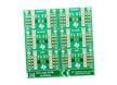
Texas Instruments 5-8-LOGIC-EVM Evaluation Module
Developed to support leaded Logic devices in the DBV, DCK, DCT, DCU, and DRL packages.
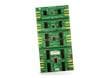
Texas Instruments AVCLVCDIRCNTRL-EVM Direction Evaluation Module
Offers support for 1, 2, 4, and 8-ch LVC and AVC family direction-controlled translation devices.