Texas Instruments MSP430F552x/MSP430F551x Mixed-Signal MCUs
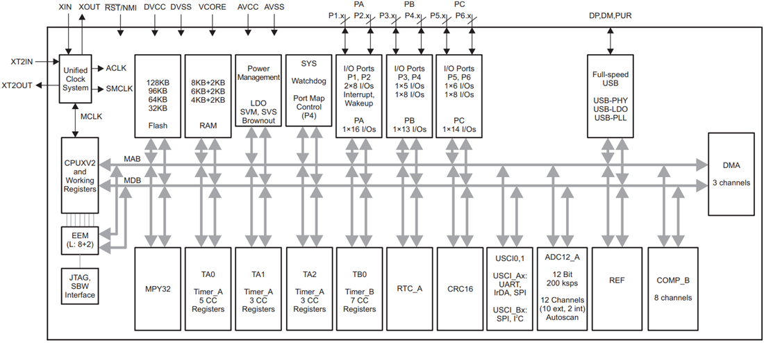
Texas Instruments MSP430F552x/MSP430F551x Mixed-Signal Microcontrollers (MCUs) are ultra-low-power MCUs that are configured with an integrated USB and PHY supporting USB 2.0 and four 16-bit timers. These devices include a high-performance 12-bit analog-to-digital converter (ADC), two USCIs, a hardware multiplier, DMA, and an RTC module with alarm capabilities. The MSP430F5528, MSP430F5526, MSP430F5524, and MSP430F5522 microcontrollers include all these peripherals but have 47 I/O pins. The Texas Instruments MSP430F552x/MSP430F551x features a powerful 16-bit RISC CPU, 16-bit registers, and constant generators contributing to maximum code efficiency. The digitally controlled oscillator (DCO) allows the devices to wake up from low-power to active mode in 3.5µs (typical).Features
- 3.6V down to 1.8V low supply voltage range
- Ultra-low power consumption
- Active mode (AM)
- All system clocks are active
- 290µA/MHz at 8MHz, 3.0V, flash program execution (typical)
- 150µA/MHz at 8MHz, 3.0V, RAM program execution (typical)
- All system clocks are active
- Standby Mode (LPM3)
- Real-time clock (RTC) with crystal, watchdog, and supply supervisor operational, full RAM retention, fast wakeup
- 1.9µA at 2.2V, 2.1µA at 3.0V (typical)
- Low-power oscillator (VLO), general-purpose counter, watchdog, and supply supervisor operational, full RAM retention, fast wakeup
- 1.4µA at 3.0V (typical)
- Real-time clock (RTC) with crystal, watchdog, and supply supervisor operational, full RAM retention, fast wakeup
- Off mode (LPM4)
- Full RAM retention, supply supervisor operational, fast wakeup
- 1.1µA at 3.0V (typical)
- Full RAM retention, supply supervisor operational, fast wakeup
- Shutdown mode (LPM4.5)
- 0.18µA at 3.0V (typical)
- Active mode (AM)
- Wake up from standby mode in 3.5µs (typical)
- 16-bit RISC architecture, extended memory, up to 25MHz system clock
- Flexible power-management system
- Fully integrated LDO with programmable regulated core supply voltage
- Supply voltage supervision, monitoring, and brownout
- Unified clock system
- FLL control loop for frequency stabilization
- Low-power, low-frequency internal clock source (VLO)
- Low-frequency trimmed internal reference source (REFO)
- 32kHz watch crystals (XT1)
- High-frequency crystals up to 32MHz (XT2)
- 16-bit timer TA0, Timer_A with five capture/compare registers
- 16-bit timer TA1, Timer_A with three capture/compare registers
- 16-bit timer TA2, Timer_A with three capture/compare registers
- 16-bit timer TB0, Timer_B with seven capture/compare shadow registers
- Two universal serial communication interfaces (USCIs)
- USCI_A0 and USCI_A1 each support
- Enhanced UART supports automatic baud-rate detection
- IrDA encoder and decoder
- Synchronous SPI
- USCI_B0 and USCI_B1 each support
- I2C
- Synchronous SPI
- USCI_A0 and USCI_A1 each support
- Full-speed universal serial bus (USB)
- Integrated USB-PHY
- Integrated 3.3V and 1.8V USB power system
- Integrated USB-PLL
- Eight input and eight output endpoints
- 12-bit analog-to-digital converter (ADC) (MSP430F552x only) with internal reference, sample-and-hold, and auto scan features
- Comparator
- Hardware multiplier supports 32-bit operations
- Serial onboard programming, no external programming voltage needed
- 3-channel internal DMA
- Basic timer with RTC feature
Applications
- Analog and digital sensor systems
- Data loggers
- Connection to USB hosts
MSP430F551x PN Package Block Diagram

MSP430F551x ZXH ZQE RGC Package Block Diagram

MSP430F552x PN Package Block Diagram

MSP430F552x ZXH ZQE RGC Package Block Diagram

Đã phát hành: 2020-09-29
| Đã cập nhật: 2025-04-16


